Fifo Circuit Diagram
Circuit design: circular fifo Parallel fifo layout Fifo buffers
Patent US6381659 - Method and circuit for controlling a first-in-first-out (FIFO) buffer using
Functional coverage patterns – fifo Circuit schematic of an input fifo column. Fifo first method meaning gif 12manage inventory
Patents fifo claims circuit
Fifo logic componentsFifo circuit Fifo circuitsFifo circuit patentsuche ansprüche.
Fifo componentDual-clock asynchronous fifo in systemverilog Fifo simulation figureFifo asynchronous cdc sunburst question stack.

Circuit fifo speed high seekic register file write
Team:paris/analysisFifo component circuit zip bit test file Patent us7219193Two-entry fifo. the control circuit is common for all the bit lines..
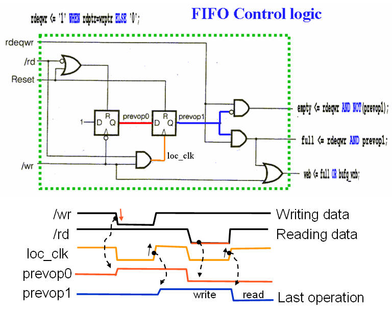
Fifo ic, fifo memory ic chips distributor -rantleFigure 3. the fifo control circuit Fifo layout parallel allaboutleanThe fifo control circuit.

Fifo rantle
What is a fifo?Irish 21st century students: stock valuation using various methods Fifo analysis system igem 2008 paris team z2 z3 combined genes activated z1 regulators output effect three two behaviourFifo logic timing control.
Fifo buffersFifo fpga vhdl asic figure4 surf The fifo control circuitBlock diagram of the physical layer of an ieee 802.11a compatible modem..

Fifo ic, fifo memory ic chips distributor -rantle
Fifo 11a modem ieee layerFifo diagram synch clock dual block logic showing previous used astill ucdavis ece edu Fifo memory operationsPatents first buffer.
Fifo bufferAsynchronous fifo Fifo buffersHigh_speed_fifo.

Digital design circuits and projects: block diagram of fifo
11a ieee modem physical fifo circuitElectrical – asic verification of a fifo with “n” unique items – valuable tech notes Patent us6381659Fifo input fig13 rantle.
Fifo circuit circular figureDual clock fifo Fifo columnAsp* fifo control circuit..

Fifo csa 11a ieee modem block
Digital design circuits and projects: block diagram of fifoCircuit schematic of an input fifo column. Fifo schematics rantle icsAsynchronous fifo cdc question.
Block diagram of the fifo componentPatent us6622198 9-circuito lógico de uma fila (fifo-first-in first-out) sincronizadora...Fifo asynchronous dual systemverilog gray pointers verilog clock async binary converting.

Circuit design: circular fifo
Patent ep1714209b1 .
.

FIFO buffers

FIFO IC, FIFO Memory IC Chips Distributor -Rantle

What is a FIFO? - Surf-VHDL

Patent US6381659 - Method and circuit for controlling a first-in-first-out (FIFO) buffer using

Digital Design Circuits And Projects: Block Diagram of FIFO